


Evolvable Hardware Lab 1
The first Lab of the Evolvable Hardware module will familiarise you with an FPGA development board. A Xilinx MicroBlaze microprocessor will be used to implement a GA that will evolve a circuit within the FPGA fabric. You will be given a basic GA to evolve a 1-bit adder, then you will adjust the code to evolve a 2-bit adder.
Setting Up
Aims: Connect up the XUP-V2Pro board, use iMPACT to configure a simple circuit and check board connectivity.
Configuration data is written to the FPGA via the board's USB port. Use a USB cable to connect the board to the extension socket above the PC monitor.

XUP-V2Pro USB Configuration Port
Data from the FPGA will be sent to the PC using the serial port. Connect the board's serial port to the serial cable provided.
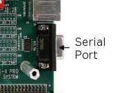
XUP-V2Pro Serial Port
To test communications with the board, we'll configure the FPGA with a simple test circuit. First we need to power-up the board. The power connector and switch are on the top-left of the board. Three power indicator LEDs should light at the top of the board. There will also be a flashing red LED, this is OK, and can be ignored.

XUP-V2Pro Serial Power Connector and Switch
Starting iMPACT
iMPACT is the Xilinx program used to configure their FPGAs. iMPACT will request a bit file with which to configure the FPGA. A test configuration bitstream can be downloaded using this link:
Linux
From the GNOME applications menu, select Course->Year 4->EHW Shell. iMPACT is started with the impact command.
> impact
Windows
Start iMPACT from Start->Programs->Hardware Development->Xilinx ISE 9.1i->accessories->iMPACT.
Once iMPACT has started, follow these steps to configure the board:
- If iMPACT complains about a 'iMPACT Access Permission', just click OK.
- When asked to load or create a project, just click cancel.
- Start the configuration process, select Edit->Launch Wizard.
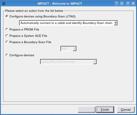
The iMPACT Wizard Dialog 1
- Make sure the dialog box matches the screenshot above, then click Finish.
- iMPACT will now try to determine what components are available for configuration. If this succeeds iMPACT will show three devices connected in a chain. If this doesn't happen, ask for help!
- The first two devices are other configurable ICs on the board's configuration chain. We need to bypass these, so click the bypass button on the first two 'Assign New Configuration File' dialog boxes.
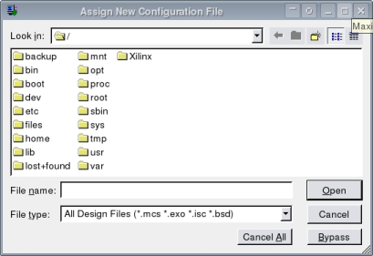
The iMPACT Wizard Dialog 2
- The last device on the chain is the FPGA, select the previously downloaded bit file,
LEDTest.bitand click Open. - Click OK on the following dialog box.
The figures below show the XUP-V2Pro configuration chain.
The XUP-V2Pro JTAG Path |
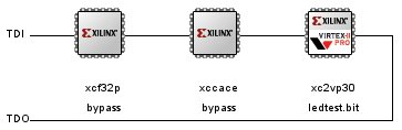
The XUP-V2Pro JTAG Chain |
- To configure the FPGA right click on the xc2vp30 device, the last on the chain, and select 'Program'.
- Select OK on the final dialog box.

If you get this, everything is OK |

If you get this, ask for help |
If the LEDs on the board are counting then everything is OK and you are ready to go on.
The Configurable Cell Array
Aims: Detail the Configurable Cell Array.
The lab involves using an array of configurable cells to evolve a 1-bit and then a 2-bit adder circuit. The circuit and truth table for a 1-bit full adder is shown below. The circuit for a 2 bit adder is also shown.
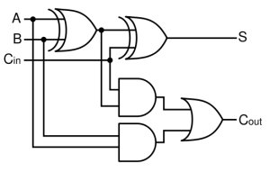
1 bit Full Adder Circuit |
|
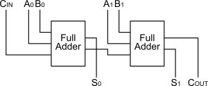
2 bit Adder Circuit |
The Configurable Cell
A basic schematic of the configurable cell is shown below. It has a 16-bit input and a 1-bit output. The LUT (look up table), shown in green, provides the logic operation. The three multiplexers, shown in yellow red and blue are used to select the inputs to the LUT. So, each LUT input can be driven from 1 of a set of 16 inputs.
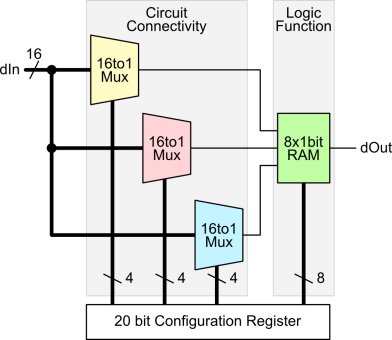
The Configurable Cell |
|
In total, this configurable cell requires 20 configuration bits. Each multiplexer requires 4 selection bits. The LUT has 8 selectable outputs.
The order of the cell's 20 configuration bits is shown in the figure below. This could be considered as a single gene in a evolutionary algorithm.
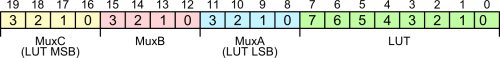
The Configurable Cell Config Bits
The Configurable Circuit
The configurable circuit is created from an array of these cells. The array is shown below. Each cell input is connected to the outputs of the two previous columns. For the special case of the first column, the previous + 1 inputs are in fact connected to an inverted form of the cell array inputs.
As there are 8 rows per column, a complete column has 8 output bits. Therefore as the multiplexers in each cell have 16 inputs, they are able to select from two columns worth of outputs.
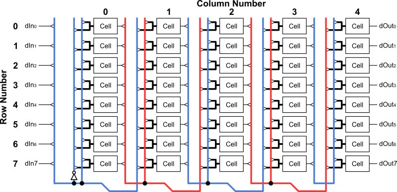
The Configurable Cell Array
Total number of configuration bits = 5 * 8 * 20 = 800 bits
With the correct configuration, the cell array can be configured to implement the adder circuits. It is the evolutionary algorithm's job to search for this configuration.
The EvoBlock Module
Aims: Detail the EvoBlock, the hardware section of the evolutionary system.
The EvoBlock Module Structure
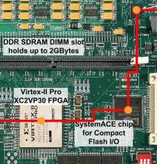
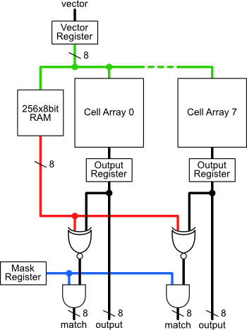
The cell array provides us with a method of testing candidate circuit solutions as part of an evolutionary algorithm. A major advantage of performing fitness evaluations in hardware is that performing multiple evaluations in parallel can be achieved quite simply. In fact 8 cell arrays have been combined into a single block called the EvoBlock. The EvoBlock also contains extra circuitry to help determine the fitness of an individual.
The figure to the left shows the basic parts of the EvoBlock Module. The block of RAM is used to store the truth table of the target circuit (in this case the 1-bit then the 2-bit adder). When test vectors are applied to the EvoBlock the correct output value is output from the RAM. This can then be compared to the output from each cell array.
The direct output from each cell array can be read, but a match output, is also generated. This output shows which bits of the RAM output and the cell array outputs match, i.e. which bits are correct. The xnor gate outputs a '1' on a match and a '0' when the bits differ. This operation is shown in the truth table below.
| RAM output | Cell Array Output | xnor output |
|---|---|---|
| 0 | 0 | 1 |
| 0 | 1 | 0 |
| 1 | 0 | 0 |
| 1 | 1 | 1 |
To determine how many bits the current individual has correct for a particular input vector, you just need to count the number of 1s in the match output.
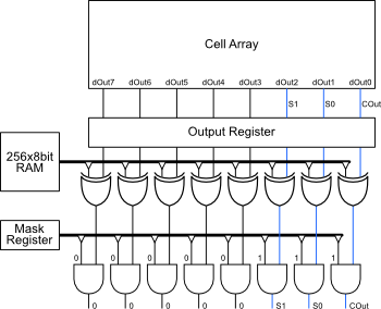
The Mask Register Connections
The final feature of the EvoBlock is the mask register. This is shown in more detail in the figure to the left.
The mask register is used to mask out unwanted outputs from the match result. This is used when
the circuit being evolved does not make use of all 8 cell array outputs. For example the 2-bit adder
only has three outputs, S1, S0 & Cout, so if these signals map
to cell array outputs dOut2 to dOut0, the mask
register will be loaded with 0x7. The match values for bits 7 down to 3 will always be '0'.
Evolving a 1-bit Adder
Aims: Use the evolutionary system to evolve a 1-bit Adder. Get an understanding of the GA code.
The evolutionary system has been developed using Xilinx's EDK software. This allows you to create embedded systems with both hardware and software elements. In our case, this is a MicroBlaze soft core (for performing the GA) and the EvoBlock (for evaluating candidate solutions). This system is shown in the figure below. The system also includes a serial UART (Universal asynchronous receiver/transmitter) so the GA can send results back to a PC.
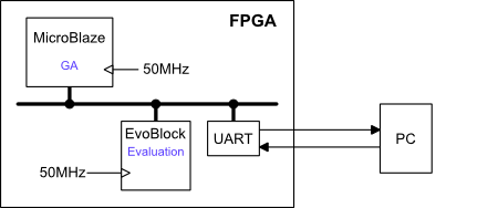
The Evolutionary System
Serial Data Monitoring
Linux
If using a Linux based system, it is possible to read the serial data directly within a terminal. The stty
command will set up the serial port, cat is used to output the serial data to the terminal.
> stty -F /dev/ttyS1 115200
> cat /dev/ttyS1
By using the tee command, it is possible to log the data as well as output it to the terminal, grep
can then be used in a different terminal to filter the data leaving the solution information.
> cat /dev/ttyS1 | tee dataLog
> tail -f dataLog | grep Solution
Windows
To monitor the output from the GA you will need a program to read data from the serial port. Download and start the program linked to below. You will need to set the configuration options so that it reads the serial packets in the same format in which they are sent. Use the image and settings listed below as a guide. Click 'Connect' to open the connection.
- Com Port 2
- 115200 Baud
- Set CR=LF
- 8 Data bits
- No Parity
- 1 Stop Bit
- No Handshaking
- Use Set Font to select 'courier new', this will make the columns easier to read.
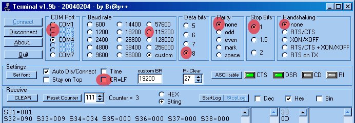
Bray Terminal
System Download
The 1-bit adder project has been built for you and can downloaded using the link below
Once downloaded, you'll need to extract the project. Make sure that the
files are extracted to a location that contains no spaces. The
project is quite large, so you might want to store it locally in tmp
rather than in your home directory.
Linux
Unzip the project using the unzip command
> unzip LogicEvolver.zip
Windows
You can use WinZip or Window's built in zip tools.
Opening EDK and the Evolution System
Linux
> xps
Windows
Start an EDK session using the desktop icon:

Xilinx Platform Studio icon
When Xilinx Platform Studio starts, you will be presented with a dialog that
allows you to create a new project or open a previously built system. Select Open
a recent project and select OK. Next navigate to where you extracted the
LogicEvolver files and select the system.xmp file
To get an idea of how the FPGA has been setup, select Project->Generate
and View Block Diagram. This loads a diagram of the FPGA system. The MicroBlaze microprocessor
can be seen at the top of the diagram. Various blocks are connected to
the core via a set of busses. The EvoBlock can be seen, named
opb_evoblock.
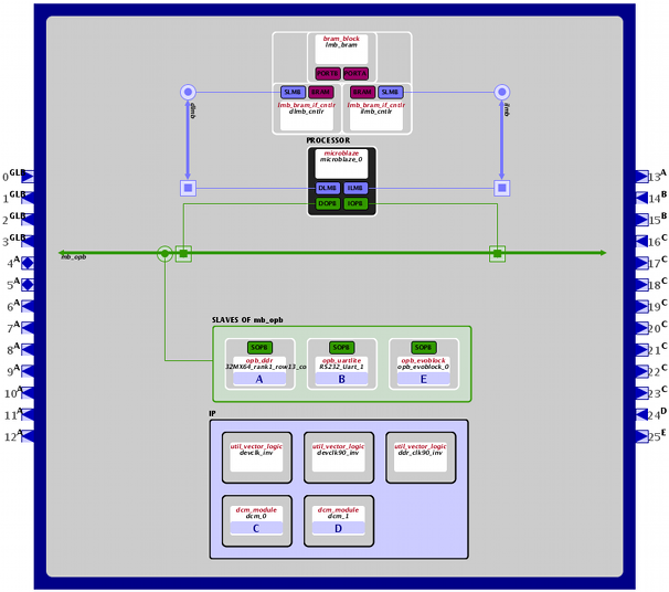
Evolution System Block Diagram
To start evolving a 1-bit adder, select Device Configuration->Download Bitstream. This makes XPS compile the project and configure the FPGA. XPS invokes iMPACT for you so you don't have to go through the process at the start of the lab. Device configuration can also be started using the toolbar icon highlighted in the figure below.
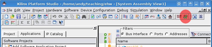
The XPS Device Configuration Toolbar button
If everything has worked, you should see messages appearing on the serial port monitor program. An example of the output is shown below.
Population size: 128, tournamentSize: 5, mutationRate: 2
Gen:   0, fittest:  10 (304), Config: 000AEA95, leastFit: 111 (200), average 255
Gen:   1, fittest:  76 (316), Config: 000FEE7B, leastFit:  58 (230), average 268
Gen:   2, fittest:  48 (319), Config: 00028CB1, leastFit: 115 (234), average 277
Gen:   3, fittest:  87 (328), Config: 0007E11D, leastFit:  41 (211), average 286
Gen:   4, fittest: 107 (333), Config: 0007A11D, leastFit:  91 (208), average 296
Gen:   5, fittest: 111 (339), Config: 000FEE7B, leastFit:  66 (236), average 305
Gen:   6, fittest:  50 (344), Config: 000FEE7B, leastFit:  66 (243), average 309
Gen:   7, fittest:  37 (366), Config: 000FEE7B, leastFit:   9 (248), average 311
Gen:   8, fittest:  67 (366), Config: 0005A11D, leastFit:  16 (212), average 313
Gen:   9, fittest:   0 (362), Config: 0007B11D, leastFit:   9 (206), average 313
The output above shows the results from the first 10 generations of the evolutionary process.
Gen:The generation number.fittest:The number of the fittest individual and its fitness in brackets.config:The configuration of the first cell of the fittest individual.leastFit:The number of the least fit individual and its fitness in brackets.average:the average population fitness.
Finding Solutions
If a solution is found, the configuration for the cell array is displayed. For this simple problem the GA should easily find a solution. The maximum fitness for the 1-bit adder is 16. As there are 8 (23=8) input vectors, and two required outputs, the total number of correct output bits is 2*8=16.
Solution Found, Gen: 101, fittest:  14 (512)
Cell  0 config: 0000A2DB
Cell  1 config: 000E5C28
Cell  2 config: 00058BF0
...
Cell 37 config: 000D4B82
Cell 38 config: 0004887E
Cell 39 config: 000A5D66
Now we are at this stage, you need to get a better understanding of how the GA code is written. The main part of the GA is in the file exp1.c. This can be opened within XPS or using an external editor.
To open in XPS, select the Applications tab, expand the 'Sources' branch, then double click the exp1.c file. Alternatively, the file can be found in the project's 'code' directory.
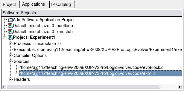
The XPS Applications Tab
Things to look out for in the code:
- A set of defines at the top specify a number of evolutionary options.
- As the EvoBlock contains 8 cell arrays, a set of 8 individuals is evaluated at a time.
- Two population arrays are used, pop1 & pop2. These are switched between being the current population, and a place to construct the next population.
The figure below shows how the cell array inputs and outputs are configured. For this 1-bit adder, only 3 inputs and 2 outputs are used.
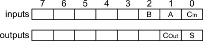
Cell Array connection for the 1-bit adder
Evolving a 2-bit Adder
Aims: To develop the GA to evolve a 2-bit Adder.
The last stage of the lab is to adjust the 1-bit adder code, to evolve a 2-bit adder. Below is a list of things to consider. The function reference section at the end of this page will help.
- Adjust the target truth table loaded into the RAM.
- Adjust the mask register.
- Change the number of applied test vectors.
- Change the MAX_FITNESS define.
This is a suggested connection plan for the cell array inputs and outputs.
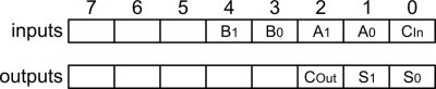
Cell Array connection for the 2-bit adder
Things to Try
The remainder of the lab gives you the opportunity to try different evolutionary techniques. Some suggestions of things to try are given below. You should try to test as many of these as possible.
- Mutation
- Rather than using a static mutation rate, try adjusting the level of mutation depending on the individual's fitness.
- Elitism
- Basic elitism, carrying the fittest unaltered to the next generation.
- A mutated elite, using a small mutation value.
- An elite selected from a pool of the best solutions so far.
- Crossover
- Crossover at the cellular level, crossing the configuration bitstream at the cell boundary.
- Lower level crossover, crossing the configuration bitstream within cell configurations.
- Representation
- The search space can be reduced by constraining the number of LUT configurations that the EA can use.
- Simplification
- Adjust the fitness measure to take into account the complexity of the solution. For example, use evolution to maximise the number of '0' bits within a working solution's configuration.
- Different Targets
- How about a 3-input adder?
Function Reference
Below is a description of the evoBlock.h and evoBlock.c files. These
are used to help with interfacing with the EvoBlock module and to perform various evolutionary
tasks.
evoBlock.h
Defines#define NUM_CELLS 40 #define NUM_CONFIG_BITS 20
NUM_CELLS defines the number of cells in the array, in this case 5 columns * 8 rows = 40.
NUM_CONFIG_BITS is the number of bits used to configure a cell, in this case 20 bits.
typedef struct
{
	Xuint32 cellConfigs[NUM_CELLS];
	Xuint32 fitness;
} ArrayConfig;
The ArrayConfig structure holds the configuration for a complete array. It also has a member to hold the
configuration's fitness. A 32 bit unsigned int is used to hold a cell's config data, however, you'll only
be using the first 20 bits of this data.
void EVOBLOCK_writeArrayNum(Xuint32 data)
Set the array number register. This selects which array will be written to when using the EVOBLOCK_writeConfig macro.
void EVOBLOCK_writeCellNum(Xuint32 data)
Set the cell number register. This selects which array will be written to when using the EVOBLOCK_writeConfig macro. Note that
every time a configuration is written (using EVOBLOCK_writeConfig) the cell number will automatically increment).
void EVOBLOCK_writeConfig(Xuint32 data)
Write a configuration to the cell pointed to by the array and cell number registers. Note that this function auto-increments the cell number register.
void EVOBLOCK_writeVector(Xuint32 data)
Write a test vector, this is input to the cell arrays, and causes the Target RAM to look up the correct result.
void EVOBLOCK_writeMask(Xuint32 data)
Write to the mask register.
void EVOBLOCK_writeTargetRAM(Xuint32 data)
Write to the location of the Target RAM pointed to by the vector register location. The Target RAM is where the desired truth table is stored. Note that this function causes the vector value to be auto-incremented, thus selecting the next Target RAM location.
void EVOBLOCK_setDebugLEDs(Xuint32 data)
Set the board's LEDs.
Xuint32 EVOBLOCK_readArrayNum()
Read the current value of the array number register.
Xuint32 EVOBLOCK_readCellNum()
Read the current value of the cell number register.
Xuint32 EVOBLOCK_readVector()
Read the current value of the vector register.
Xuint32 EVOBLOCK_readMask()
Read the current value of the mask register.
Xuint32 EVOBLOCK_readTargetRAM()
Read the contents of the Target RAM pointed to by the Vector register.
Xuint32 EVOBLOCK_readOutput0()
Read the cell Array output values for arrays 3 to 0.
| 31-24 | Array 3 |
| 23-16 | Array 2 |
| 15-8 | Array 1 |
| 7-0 | Array 0 |
Xuint32 EVOBLOCK_readOutput1()
Read the cell Array output values for arrays 7 to 4.
| 31-24 | Array 7 |
| 23-16 | Array 6 |
| 15-8 | Array 5 |
| 7-0 | Array 4 |
Xuint32 EVOBLOCK_readMatch0()
Read the masked match values for arrays 3 to 0.
| 31-24 | Array 3 |
| 23-16 | Array 2 |
| 15-8 | Array 1 |
| 7-0 | Array 0 |
Xuint32 EVOBLOCK_readMatch1()
Read the masked match values for arrays 7 to 4.
| 31-24 | Array 7 |
| 23-16 | Array 6 |
| 15-8 | Array 5 |
| 7-0 | Array 4 |
evoBlock.c
Functionsvoid writeCellConfig(Xuint32 arrayNum, Xuint32 cellNum, Xuint32 config)
Write a configuration to a particular cell.
void configureArray(Xuint32 arrayNum, ArrayConfig *config)
Configure a whole array. Note that a pointer is used to pass the config data to the function.
void randomiseArrayConfig(ArrayConfig *config);
Randomises the array configuration passed to the function. Note that a pointer is used to pass the config data to the function.
Bit Manipulation in C

The C Programming Language
The following small section is a reminder of some of the lower level operations you can perform in the C language. These bit manipulation techniques are especially useful when dealing with hardware interfacing.
The best reference for this sort of thing is probably The C Programming Language by Brian W. Kernighan and Dennis M. Ritchie.
Bit Shifts
This will shift the data variable 4 bits towards the MSB (Most significant Bit).
data <<= 4;
This will mask all bits except bits 2 and 3. That is bits 2 and 3 will retain their value whilst all others will be set to 0.
data &= 0x6;
This will set the 4th bit to a 1, leaving the others as they were.
data |= (1<<4);
This will clear the 6th bit to a 0, leaving the others as they were.
data &= ~(1<<6);
This will invert the 7th bit, leaving the others as they were.
data ^= (1<<7);
