


LCD Controller
This page describes a VHDL module for driving alphanumeric LCDs. It drives the very common HD44780 chip, a driver IC found on many LCD modules.
Overview
This LCD Driver module was designed with two aims in mind:
-
Simple: Make writing to the display as simple and flexible as possible.
From a hardware point-of-view, it would be simplest to connect the LCD pins directly to the microcontroller's general purpose IO (GPIO) pins. The disadvantage is you need to support the LCD protocol in software. Instead, it should be possible to write character data directly to memory locations that map to character positions.
Fast: Make updating the screen as fast as possible.
The LCD is a fairly slow device to operate. Communicating directly with the LCD over GPIO (without using interrupts) would require some long delays, during which the microcontroller is doing nothing. Instead, the microcontroller should be able to write character data without the need to pause between or after writes.
These two aims are achieved using the system below. The finite state machine (FSM) simplifies the operation by taking care of the LCD interface protocol. The off-screen buffer makes it fast, as it can accept new character data as fast as the microcontroller can write it.
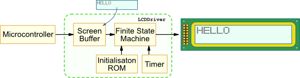
LCD Driver Overview
LCD VHDL Driver Module
The LCD driver modules makes use of the LCD's 4bit data mode. This saves IO, simplifies PCB
routing and is still fast enough for quick full screen refreshes. The port definition for the module
is shown below. To meet the LCD's timing requirements the module must be supplied with the frequency
of the clk input. This is set with the CLK_FREQ generic.
The off screen buffer is loaded using dIn, charNum and
wEn. This is a very simple interface. The screen location specified by
charNum is written with the value specified by dIn on a rising clock edge
when the wEn input is high. The module is written for a 2x20 character LCD, so the
charNum input ranges from 0 to 39. The module can be very easily adjusted for
different display sizes.
The actual LCD is connected to the driver module via lcdData, lcdRS and
lcdE. These connect directly to the LCD connections with the same name. As the module
only writes character data to the LCD, there is no need for a lcdRW signal.
LCDDriver4Bit.psmentity LCDDriver4Bit is generic (CLK_FREQ : positive); -- Frequency of clk input in Hz port ( clk : in std_logic; reset : in std_logic; -- Screen Buffer Interface dIn : in std_logic_vector(7 downto 0); charNum : in integer range 0 to 39; wEn : in std_logic; -- LCD Interface lcdData : out std_logic_vector(3 downto 0); lcdRS : out std_logic; lcdE : out std_logic); end LCDDriver4Bit;
Download the module using the link below.
Note: This design continually updates the LCD module, even if the off screen buffer (within the FPGA) does not change. This is not particularly efficient. However, if you're worried about power consumption or excessive IO traffic, it would be a simple modification to the VHDL in order to only update the LCD module when the off screen buffer has been changed.
Xilinx PicoBlaze Example
The LCD driver module is very easy to interface to the Xilinx PicoBlaze microcontroller core. The example system shown below is based on the Digilent Nexys 2 Development Board, but is easily used with other setups.
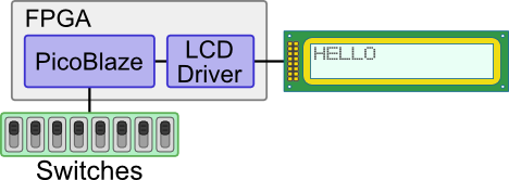
LCD Driver connected to Xilinx PicoBlaze |
LCD connected to Digilent Nexys |
The PicoBlaze code shown below reads in the state of the switches and uses this value to set the value in the LCD character screen buffer. The LCD Module then takes care of writing this to the actual display.
lcd.psm; Simple LCD Test code CONSTANT LCD_CHARNUM, 00 CONSTANT LCD_DATA, 02 CONSTANT SWITHCES, 01 init: load s0, 00 ; Initialise address reg to zero loop: output s0, LCD_CHARNUM ; Write LCD Char Address input s1, SWITHCES ; Read Switches output s1, LCD_DATA ; Write LCD Data add s0, 01 ; Increment address compare s0, 28 ; Check for address 40 (0x28) jump NZ, loop load s0, 00 ; Reset address to zero jump loop
Here are the files:
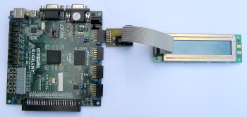
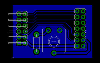
Interface PCB
Below is a simple PCB for interfacing the LCD to a Digilent Nexys2 FPGA development board. The pot is used to set the LCD's contrast.
|
|
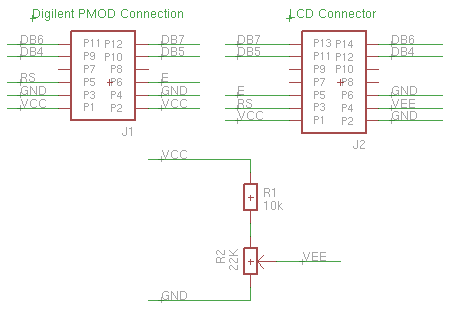
Below is the connections for the Nexys2 JA1 IO port (the connector nearest the power socket). Note: the connector pin numbers differ between the development board header and the interface PCB header. Next to it is a pin diagram for the LM032XMBL LCD module.
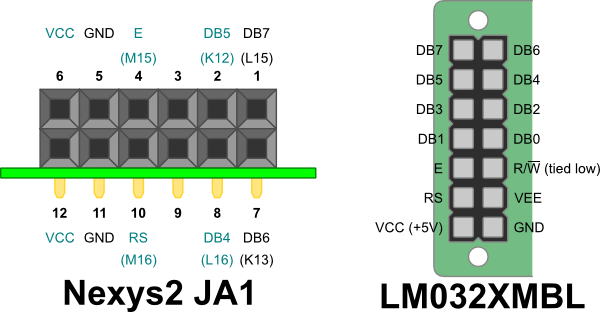
Note: The LCD uses 5V IO whereas the FPGA uses 3.3V IO. As the LCD is only being written to, level translation is not required, as the 3.3V output signals can drive the 5V inputs, with a slight loss in noise immunity.
Further LCD Information
