


Digilent XUP-V2Pro
This page contains a number of resources for the XUP-V2Pro FPGA Development Board.
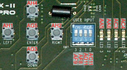
Push Buttons, Switches & LEDs
Push Buttons
| Button Label | Button Number | FPGA Pin Label | FPGA Pin Number |
|---|---|---|---|
| ENTER | SW2 | IO_L02N_3 | AG5 |
| UP | SW3 | IO_L04P_3 | AH4 |
| DOWN | SW4 | IO_L04N_3 | AG3 |
| LEFT | SW5 | IO_L03N_3/VREF_3 | AH1 |
| RIGHT | SW6 | IO_L02N_3 | AH2 |
Note: The push switches use pull-up resistors, therefore when released their output is high, when pressed their output is low.
Switches
| Number (On PCB) | FPGA Pin Label | FPGA Pin Number |
|---|---|---|
| 0 | IO_L37N_4 | AC11 |
| 1 | IO_L37P_4 | AD11 |
| 2 | IO_L38N_4 | AF8 |
| 3 | IO_L38P_4 | AF9 |
LEDs
| LED Label | LED (Diode) Number | FPGA Pin Label | FPGA Pin Number | EDK GPIO bit |
|---|---|---|---|---|
| LED_3 | D7 | IO_L44N_3 | AA5 | 0 |
| LED_2 | D8 | IO_L44P_3 | AA6 | 1 |
| LED_1 | D9 | IO_L43N_3 | AC3 | 2 |
| LED_0 | D10 | IO_L43P_3 | AC4 | 3 |
Note: Board LEDs are switched on with a logic 0 and off with a logic 1.
Push Buttons
Clock Sources
| Clock | Frequency/ Period |
PCB Signal Name |
FPGA Pin Label |
FPGA Pin Number |
Device PCB Label |
Notes |
|---|---|---|---|---|---|---|
| System Clock | 100 MHz/ 10ns |
SYSTEM_CLOCK | IO_L75P_4/GCLK0P | AJ15 | Y2 | |
| Alternate Clock | ALTERNATE_CLOCK | IO_L75P_5/GCLK6P | AH16 | Y3 | Unpopulated | |
| High Speed Module Clock | HSCLK_IN | IO_L74P_0/GCLK6S | B16 | Clock from High Speed Expansion Module | ||
| MGT Clock | 75 MHz/ 13.333ns |
MGT_CLK_P | IO_L75P_0/GCLK4S | F16 | U10 | Bottom side of PCB |
| MGT_CLK_N | IO_L75N_0/GCLK5P | G16 | ||||
| External Clock | EXTERNAL_CLOCK_P | IO_L75P_1/GCLK2S | G15 | J23 | Unpopulated Connector | |
| EXTERNAL_CLOCK_N | IO_L75N_1/GCLK3P | F15 | J24 | Unpopulated Connector | ||
| System ACE Clock | 32 MHz/ 31.25ns |
FPGA_SYSTEMACE_CLOCK | IO_L75N_4/GCLK1S | AH15 | Y4 |
The footprint of the Alternate Clock pads is shown below. Note that the EN signal is connected to VCC3.3, so any inserted module will always be enabled.
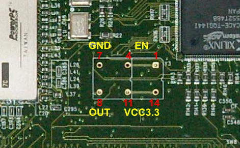
Alternate Clock Footprint
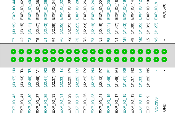
Expansion Headers
Note: There seem to be errors in the XUP-V2Pro datasheet (UG069 - v1.0).
- Page 54 Table 2-14, J5 Pin 40 is FPGA Pin T7
- Page 54 Table 2-15, Table for J6 PIN not J5 PIN
- Page 55 Same as above
- Page 56 Same as above
- Page 56 Table 2-15, J6 Pin 34 is signal EXP_IO_76
Hopefully they are correct in the diagram below.
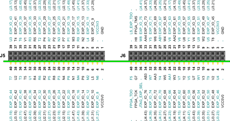
J5 & J6 Connectors
Another view of that same connections. This time looking at the PCB pads that would be place on an add-on board.
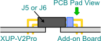
Edge Connector Diagram
J5 PCB Pads
SATA Ports
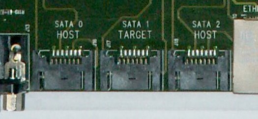
SATA Ports
| Port | Type | Signal Name | FPGA Pin Number |
|---|---|---|---|
| SATA 0 | Host | SATA_PORT0_TXP | A26 |
| SATA_PORT0_TXN | A27 | ||
| SATA_PRT0_RXP | A25 | ||
| SATA_PRT0_RXN | A24 | ||
| SATA 1 | Target | SATA_PORT1_TXP | A19 |
| SATA_PORT1_TXN | A20 | ||
| SATA_PRT1_RXP | A18 | ||
| SATA_PRT1_RXN | A17 | ||
| SATA 2 | Host | SATA_PORT2_TXP | A13 |
| SATA_PORT2_TXN | A14 | ||
| SATA_PRT2_RXP | A12 | ||
| SATA_PRT2_RXN | A11 |
High Speed Expansion Port
The J37 Header is split into two banks of 50, labelled A and B. Looking into the header, pins A1 and B1 are on the right, pins A50 and B50 are on the left. Bank A is on top, bank B is on the bottom.

J37 Connector
Bank B is mostly ground connections. Bank A contains 40 general purpose IO signals.
